Materials and devices for energy efficient spiking neuromorphic hardware
The predicted deployment in tens of billions of Edge Artificial Intelligent (Edge AI) Internet-of-Things nodes based uniquely on traditional chip technologies is facing multiple sustainability issues from the point of view of energy efficiency and of electronic waste. This talk will address the challenge of new classes of scalable neuromorphic hardware enabling energy-efficient chips designed for Edge AI and autonomous operation. The electronic functionalities and the structure of this neuromorphic hardware are greatly inspired by biological neural systems and is based on combining a few material and device innovations such as: ferroelectricity in doped high-k dielectrics, multi-gated 2D semiconducting devices, and, memristive phase change materials and devices, capable to emulate both artificial synapses and neurons.
We envision a technological effort from material to system level that will permit the integration of spiking neuromorphic hardware in the back-end-of-line (BEOL) of advanced silicon CMOS platforms, providing not only the co-integration with digital technologies but also the extension of silicon chips exploiting the 3rd dimension, preserving reduced footprints and integrating energy storage.
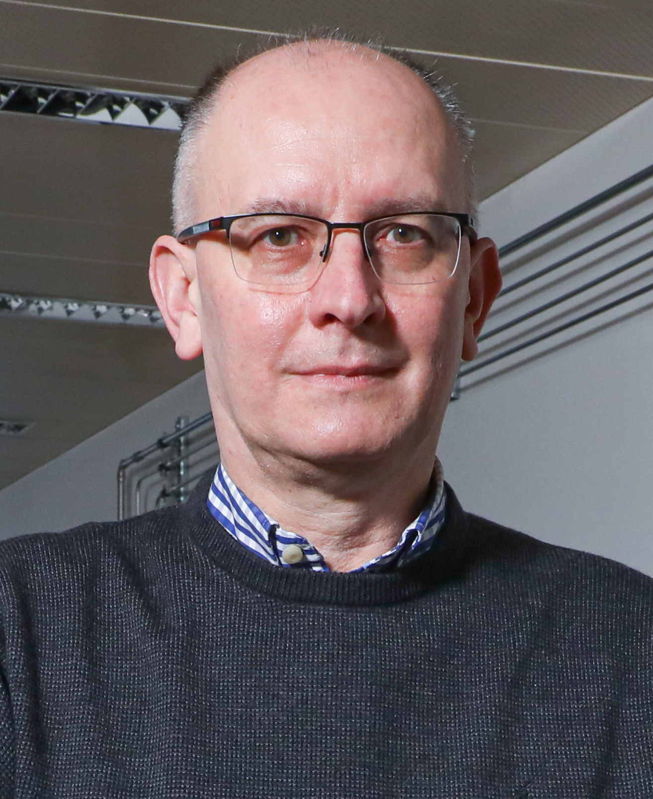
Prof. Adrian M. Ionescu, PhD, is a Full Professor of Nanoelectronics at Ecole Polytechnique Fédérale de Lausanne (EPFL), Switzerland. He received the B.S. &M.S. in Electronics and Telecommunications in 1989 from the University ‘Politehnica’ Bucharest, Romania. He holds two PhDs, in Microelectronics, from University ‘Politehnica’ Bucharest (1994) and in Physics of semiconductor devices from the National Polytechnic Institute of Grenoble, France (1997).
He is the founder and director of the Nanoelectronic Devices Laboratory (Nanolab: http://nanolab.epfl.ch/ ) of EPFL. His research deals with beyond CMOS and More-Than-Moore energy efficient devices and technologies. His group pioneered steep slope transistors, M/NEMS devices with main emphasis on low power concepts in order to achieve novel energy efficient digital, analog, radio frequency and low power sensing functions. He has been the leader of many European projects focusing on low power nanoelectronics and nanotechnology for smart systems. He was an Editor of IEEE Transactions on Electron Devices and is currently a Board Member of Proceedings of IEEE. He has served the Technical Committees of many IEEE conferences, and, he was the Technical Chair of IEEE SNW at IEEE VLSI Technology Symposium 2016 (USA), and the General Chair of the IEEE European Solid-State Devices and Circuits Research Conference (ESSDERC/ESSCIRC 2016).
Prof. Ionescu has published more than 600 articles in international journals and conference proceedings. He is the recipient of IBM Faculty Award 2013 for contributions to the Engineering and the recipient of André Blondel Medal 2009 of the Society of Electrical and Electronics Engineering, Paris, France. He and his group received the IEEE George Smith Award in 2017. He is an IEEE Fellow and in 2015 he was elected as a member of the Swiss Academy of Sciences (SATW). In the same year he received the Outstanding Achievement Award of SATW for the successful coordination and delivery of the first national Swiss Technology Outlook to the Swiss government. In 2016 he received an Advanced ERC (European Research Council) Grant for individual senior scientists in Europe to develop a program aiming at energy efficient computation and sensing for Internet-of-Things. Currently, he leads the FET Proactive DIGIPREDICT, a European Consortium developing Digital Twins for Personalized, Preventive and Participatory Healthcare, a paradigm change in future sustainable healthcare.
Evolution of MOSFETs toward nanoelectronics
We review the origins, evolution and present status of MOSFETs, which has been the dominant semiconductor device in electronics applications for more than 4 decades. The conceptual invention of MOSFET, by Lilienfeld in 1928, and the end of World War II, in 1945, inspired Bell Labs to research into semiconductors. Bardeen and Brattain, who were working in the Semiconductor Sub-Group at Bell Labs, fabricated the first point contact transistor in December,1947. This achievement motivated Shockley, who was the group leader, to invent the bipolar junction transistor in January 1948. Bardeen, Brattain and Shockley received the Nobel Prize in 1956 “for their discovery of the transistor effect.” After solving oxide reliability problems, the MOSFET was fabricated in 1960 by Kahng and Atalla. The invention of CMOS, by Wanlass and Sah in 1963, made the MOSFET to be the most commonly used device in digital applications. The transistors have been miniaturized for more than fifty years, following Moore’s Law from 1965, and they are now approaching their final limits in the nanometer regime. Recent innovations, such as strained silicon and high-k metal gates are being used in modern MOSFETs. New device designs as FinFETS, Nanowire and Nanosheet are now being fabricated.

Prof. Adelmo Ortiz-Conde, PhD, received the professional Electronics Engineer degree from Universidad Simón Bolívar (USB), Caracas, Venezuela, in 1979 and the M.E. and Ph.D. from the University of Florida, Gainesville, in 1982 and 1985, respectively.
From 1979 to 1980, he served as an instructor in the Electronics Department at USB. In 1985, he joined the technical Staff of Bell Laboratories, Reading, PA, where he was engaged in the development of high voltage integrated circuits. In 1987, he returned to the Electronics Department at USB where he was promoted to Full Professor in 1995.
He was on sabbatical leave at University of Central Florida (UCF), Orlando, from January to August 1994, and again from July to December 1998. He also was on sabbatical leave at “Centro de Investigaciones y Estudios Avanzados” (CINVESTAV) National Polytechnic Institute (IPN), Mexico City, Mexico, from October 2000 to February 2001.
He has coauthored one textbook, Analysis and Design of MOSFETs: Modeling,
Simulation and Parameter Extraction (2012 Springer reprint of the original 1st ed. 1998,
http://dx.doi.org/10.1007/978-1-4615-5415-8 ), over 190 international technical journal
and conference articles (including 20 invited review articles). His present research
interests include the modeling and parameter extraction of semiconductor devices.
Reliability of Nanoscale Semiconductor Devices, focusing on but not limited to Noise and Bias Temperature Instability
Effects that play a major role on the reliability of today digital and analog designs are discussed, as well as effects that are expected to become relevant in future technologies. Modeling techniques to abstract the physical level effects into the design flow are studied. The main focus of the talk is charge capture and emission by defects (traps) close to the Dielectric-Semiconductor interface, which is known to be the major source of low- frequency noise in modern MOS devices. It is also known to cause in Bias Temperatur Instability (BTI). The basics mechanisms involved in charge trapping and de-trapping will be presented, including a critical discussion of key parameters such as trapping/de-trapping time constants and the amplitude of the fluctuations induced by single traps. A novel physics based modeling and simulation approach will be presented. It is based on the relevant microscopic quantities that play a role in both low-frequency noise and BTI. The modeling approach is valid at both DC and large signal (AC) biasing, and may be applied to time domain (transient) and frequency domain (AC) analysis. LF-noise (and BTI) levels can vary by several orders of magnitude in deeply scaled devices, making variability a major concern in advanced MOS technologies. Therefore, to assure proper circuit design in this scenario, it is necessary to identify the fundamental mechanisms responsible for variability in LF-noise and BTI.
Time domain analysis is relevant for the analysis of digital and mixed-signal circuits. In digital circuits, the RTN chronological statistics, especially trap occupancy switching, has direct impacts on circuit performance and reliability, as degradations like jitter of signals happen when a trap switches state. The area scaling of RTN induced jitter (phase noise) and its variability is detailed and discussed, aiming to support circuit designers in transistor sizing towards a more reliable design. The applicability of the model here presented to the evaluation of logic gates and circuits composed by logic gates is studied and demonstrated by the case study of inverters and ring oscillators.
The talk is focused on nano scale MOS devices, but novel devices such as Resistive Switching Memory (RRAM/ReRAM) are also addressed.

Prof. Gilson Wirth, PhD, received the B.S.E.E and M.Sc. degrees from the Universidade Federal do Rio Grande do Sul, Brazil, in 1990 and 1994, respectively. In 1999 he received the Dr.-Ing. degree in Electrical Engineering from the University of Dortmund, Dortmund, Germany.
He is currently a professor at the Electrical Eng. Depart. at Univ. Federal do Rio Grande do Sul – UFRGS (since January 2007).
From July 2002 to December 2006 he was professor and head of the Computer Engineering Department, Univ. Estadual do Rio Grande do Sul – UERGS. His current research work focuses on modeling and electrical stimulation of charge trapping in the context of Bias Temperature Instability (BTI), Low-Frequency Noise (1/f and RTN) and Hot Carrier Degradation (HCD).He has also worked on ionizing radiation effects (TID and SET/SEU) on semiconductordevices.He focuses on collaborative work with academia and industry. He has stablished successful collaborative work with different companies and research groups in Europe, North and South America, and China. Has signed NDA with the following companies:Intel, Texas Instruments, NXP Semiconductors and Infineon.
Circuits and technologies for implantable biomedical devices
Biological processes such as neuronal signaling and cell growth are among the most complex micro- and nano-scale processes in nature. Historically such processes have been studied at system level because there were no tools available to study individual components of the process. However, cellular-level interfacing is needed to provide better understanding of the brain and to develop more advanced prosthetic devices and brain-machine interfaces. With semiconductor technology innovations, much recent work has been focused on unraveling biological complexity, but also on driving new diagnoses, treatments and therapies that are tailored to the individual. One of the drivers behind those innovations is novel CMOS circuits enabling multi-modal, high-precision data collection and analysis at ultra-low power consumption. In this talk, I will present recent biomedical developments based on silicon technology, and I will discuss the requirements, materials, circuit techniques and design challenges of their ASIC and SoC platforms.

Carolina Mora Lopez, PhD, received her Ph.D. degree in Electrical Engineering in 2012 from the KU Leuven, Belgium, in collaboration with imec, Belgium. From 2012 to 2018, she worked at imec as a researcher and analog designer focused on interfaces for neural-sensing applications. She is currently the Scientific Director and team leader of the circuits for neural interfaces team in imec. Her research interests include analog and mixed-signal circuit design for sensor, bioelectronics and neural interfaces. Carolina is a senior IEEE member and serves on the technical program committee of the VLSI circuits symposium, ISSCC and ESSCIRC conferences.
Nonlinear Photonics Based on Thin-Film Lithium Niobate
Lithium niobate (LN) is an excellent nonlinear photonic material due to its large electro-optic (EO) coefficient, second order (2) and Kerr ((3)) nonlinearity, along with a wide optical transparency window. Thanks to the recent advances in nanofabrication technology, monolithic LN waveguides with high optical confinement and ultralow linear loss has been achieved, which was critical to the success of the silicon-based platform in the past decade. Highly efficient and controllable light-matter interactions can be achieved using optical, electrical, or mechanical waves at extremely compact footprints. In this talk, I will review our recent developments of thin-film LN nonlinear devices for (2) and (3)-based parametric frequency conversion, high power EO frequency combs, femtosecond pulse synthesis and optical isolator. Combination of multiple nonlinearities of LN unlocks ultrabroadband electromagnetic spectrum from microwave to mid-infrared. Lastly, I will discuss the potential of LN photonic platform for scaling up and accelerating classical and quantum technologies in sensing, photonic computing, and communication networks.

Mengjie Yu is Gabilan Assistant Professor at the University of Southern California, Department of Electrical and Computer Engineering. She received her Ph.D. degree in Electrical and Computer Engineering in 2018 from Cornell University and held research staff associate position in Applied Physics and Mathematics at Columbia University from 2015-2018. She is a postdoctoral fellow in the John A. Paulson School of Engineering and Applied Sciences at Harvard University from 2018-2021
Her research group focuses on developing nanoscale nonlinear and quantum photonics devices for optical communication, computing, sensing, and metrology. Her research interests include nonlinear physics, optical frequency comb, spectroscopy, photonic computing, and quantum optics, enabled by advanced nanofabrication of low-loss photonic structures based on silicon, silicon nitride, and lithium niobate.
She serves on the Early Career Editorial Advisory Board for APL Photonics. She is the 2020 the Optica (formerly OSA) Ambassador, the Caltech 2019 Young Investigator Lecturer, and the Rising Star Women in Engineering in the Asian Deans Forum 2019. She served as chair of the OSA Integrated Photonics Technical Group from 2019 – 2021.

